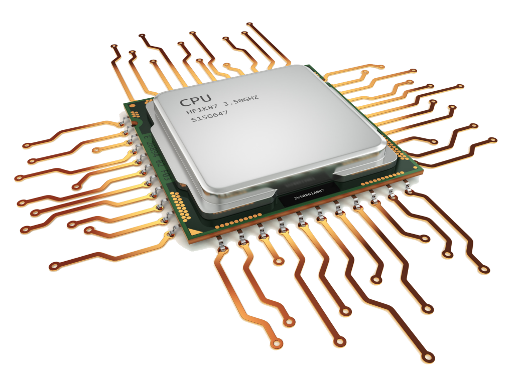

Printed Circuit Board (PCB) design is the process of planning and creating the layout of an electronic circuit that will be fabricated into a PCB. The PCB serves as the physical base that connects and supports the electronic components of a device, providing both electrical connections and mechanical support.
Designing a PCB involves several critical steps, from schematic creation to routing, simulation, verification, and ultimately, preparing files for manufacturing. Let’s break down the PCB design process and discuss the key elements involved.
The PCB Design Process
PCB design involves several key stages, from conceptualizing the circuit to preparing manufacturing files. Below is an outline of the typical process:
1. Define Circuit Requirements
- Specification Gathering: Understand the purpose of the PCB, the required functions, and the components needed.
- Component Selection: Choose components like resistors, capacitors, diodes, microcontrollers, and integrated circuits (ICs) based on performance, availability, and cost.
- Power Requirements: Estimate power consumption to ensure the PCB can handle the voltage and current requirements of the circuit.
2. Schematic Design
The schematic is a detailed diagram of the electronic circuit that defines how components are connected.
- Schematic Software: Tools like Eagle, KiCad, Altium Designer, or OrCAD are commonly used to create schematics.
- Component Placement: Position components on the schematic and wire them appropriately.
- Simulation: Simulate the circuit’s behavior to ensure that it works as expected (some tools support circuit simulation as part of the design process).
- Bill of Materials (BoM): A list of all components, their values, part numbers, and specifications, is generated during this step.
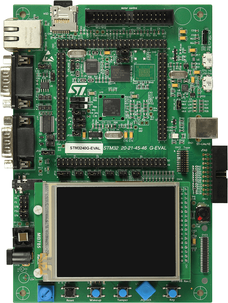
3. PCB Layout/Placement
After the schematic design, the next step is to place the components on the physical PCB layout.
- Component Placement: Use the PCB design software to arrange components on the board. The layout should consider ease of assembly, signal integrity, heat dissipation, and electrical isolation.
- Layer Planning: Plan the number of layers (single-layer, double-layer, or multi-layer) based on the complexity of the design.
- Top Layer: Components and power planes are typically placed here.
- Bottom Layer: Components or additional traces may be placed here.
- Inner Layers: Used in multi-layer PCBs to route signals and power through vias.
4. Routing (PCB Traces)
Once the components are placed, the next step is routing the electrical connections between components using copper traces.
- Trace Width and Spacing: Define the trace width based on current requirements (using IPC-2221 or similar standards). Ensure proper spacing to avoid short circuits.
- Via and Layer Transitions: Use vias (vertical interconnects) to connect traces between different layers of a multi-layer PCB.
- Signal Integrity: For high-frequency circuits, it’s critical to maintain signal integrity. This might involve controlled impedance, minimizing via usage, and keeping traces short and direct.
5. Design Rule Check (DRC)
Once the PCB layout is complete, perform a Design Rule Check (DRC) to ensure that the design adheres to the manufacturing constraints.
- DRC Software: PCB design tools automatically run DRC checks to validate trace widths, component clearances, hole sizes, and other manufacturing rules.
- Electrical Rule Check (ERC): This ensures there are no logical errors in the design, like unconnected pins or incorrect connections.
6. Simulation and Testing
In some cases, PCB designers may run simulation software to validate the behavior of the PCB before moving to the physical manufacturing stage.
- Signal Integrity: Simulate signal integrity to identify issues like noise, cross-talk, and ground bounce.
- Thermal Analysis: Some designs may require thermal simulation to ensure that heat dissipation is effective and that high-power components don’t overheat.
7. Generate Gerber Files
After finalizing the PCB design, the next step is to generate the Gerber files, which are the standard format for PCB manufacturing.
- Gerber Files: These files contain all the necessary details for manufacturing the PCB, including copper traces, holes, silkscreen, and solder mask layers.
- Drill Files: Separate files are generated for the holes or vias, specifying the size and position for drilling.
- Assembly Files: These files include the location of components for placement during the assembly process.
8. PCB Fabrication and Assembly
- PCB Fabrication: Send the Gerber files to the PCB manufacturer, who will fabricate the PCB based on the design specifications (layer stacking, copper thickness, surface finish, etc.).
- Assembly: After fabrication, components are soldered onto the PCB, either manually or using automated processes like Pick-and-Place machines.
- Testing: The assembled PCB is tested using automated testing methods like In-Circuit Testing (ICT) or Functional Testing to ensure everything works as intended.